All the latest quantum computer articles

See the latest stories on quantum computing from eeNews Europe

Friday, June 30, 2017

Top stories in June on the Embedded Blog

By Nick Flaherty www.flaherty.co.uk

It's poignant farewell to Intel's Quark processor in the IoT world for me here at the Embedded blog, as Wikipedia use one of my stories on the device as a reference for their entry on the chip. But I never understood why they chose to use the Pentium II architecture rather than modify the more modern developments (which they did with the Atom E3800 which is now the mainstay for IoT). Oh well.

We are also still waiting for the report that may shed some light on the bizarre catastrophe at Bristish Airways with their data centre power system. None of the explanations ring true, because if they actually ARE true, it was a disaster waiting to happen from an archaic and frankly negligent system architecture.

But its good the see the popularity of a self-powered Bluetooth mesh network as the most popular post this month (although being the first one this month definitely helps!) - EnOcean is finally coming alongside the existing standards as well as its own, which will bring its technology to a much wider market.

EntryPageviews
161
158
154
147
147
144
142
138
131


Thursday, June 29, 2017

First ARM Based COM Express Type 7 module for Telco networking

By Nick Flaherty www.flaherty.co.uk

Israeli embedded module developer SolidRun has launched the industry's first COM Express Type 7 module based on the ARM architecture. 

With two 10 Gigabit Ethernet ports, the $300m CEx7 A8040 module targets high-speed network applications in data centres, internet protocol appliances, network function virtualization (NFV), unified control and data planes, software defined networking, secured routers, and virtual customer premises equipment.

The module is based on the Armada 88F8040 quad-core ARM Cortex-A72 processor from Marvell and supports up to 2GHz CPU clock speed with symmetrical multiprocessing operation modes. This supports two 10 Gigabit Ethernet ports, and one standard Gigabit Ethernet port with on board 64-bit DDR4 (up to 16GB) and ECC for mission critical applications. 

The module also supports on board NOR Flash and NAND Flash eMMC based storage and has four PCIe 3.0 lanes, two SATA ports and two USB 3.0 ports. For integration of additional peripherals, the board features eight GPIO/SDIO interfaces, two serial communications interfaces and supports both SPI and i2C bus protocols.

SolidRun is using the module and carrier card for the ClearFog 8040 that provides networking and connection features, including dual 10GbE, two M.2 connectors supporting both SATA and NVME SSDs, MicroSD socket and two USB 3.0 connectors. This is the highest bandwidth single board computer in its category, says the company.

"Our new CEx7 8040 COM module is a powerful addition to the range of solutions we provide," states Dr. Atai Ziv, SolidRun's CEO. "The combination of robust processing abilities with strong networking capabilities offers a variety of applications with a focus on network infrastructure. Also, the COM Express Type 7 form factors allows for simpler deployment options."

The CEx7 A8040 will initially be offered in two form factors; CEx7 A8040 Basic (125mm X 95mm) and the CEx7 A8040 Mini (84mm X 55mm), alongside the ClearFog 8040 Single Board Computer.

www.solid-run.com

Toshiba squeezes 1.5Tbytes of data into one package (and releases a 1TB embedded drive)

By Nick Flaherty www.flaherty.co.uk

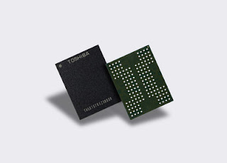
Multi-level NAND flash is not a great technology for many embedded designs, but Toshiba has managed to stack 16 high density die into a package that stores 1.5Tbits of data.

The latest BiCS device uses a 4-bit-per-cell, quadruple-level cell (QLC) technology for the first time that enables larger die capacity than the company's third-generation 512Gb 3-bit-per-cell, triple-level cell (TLC), and pushes the boundaries of flash memory technology using a 64-layer stacked cell structure. This achieves the world's largest die capacity at 768Gbits/96GBytes. This is up from 128Gbytes in a package back in 2011.

The QLC flash memory also enables a 1.5-terabyte (TB) device with a 16-die stacked architecture in a single package, up 50% on the 1TByte package.

Increasing the number of bits-per-cell by one within the same electron count requires twice the accuracy of TLC technology, and Toshiba has combined its advanced circuit design and leading 3D flash memory process technology to overcome this challenge, successfully creating the world's first QLC 3D flash memory.

This could be especially beneficial for datacentre designs. 

"The introduction of QLC technology sets the stage for solving many of the challenges facing datacentres today," said Greg Wong, founder and principal analyst at Forward Insights. "For datacentres, QLC SSDs can be an excellent design choice for reducing power consumption and lowering footprint. Additionally, as the push for higher capacity HDDs leads to an increase in areal density and drives up the weight per successive generation, it has become common to see a 42U rack only half-filled due to exceeding maximum weight or power supply. Flash memory-based storage solutions weigh less and give improved power efficiencies, enabling datacentres to achieve greater rack capacity."

"From SLC to MLC and MLC to TLC, large technology shifts are often met by industry resistance and the introduction of QLC is no exception," said Scott Nelson, senior vice president of Toshiba America's memory business unit, which competes with Samsung. "There will always be demand for compelling storage solutions that bring higher densities and produce a favourable cost/performance equation – our QLC technology falls squarely into that sweet spot. History has proven us right in the past when it comes to our visionary flash memory roadmap, and we fully expect QLC BiCS FLASH to continue our industry-leading track record."

Samples began shipping this month to SSD and SSD controller vendors for evaluation and development. 

Toshiba Memory Blog

Update - 30th June

Toshiba has also launched a new line of NVM Express (NVMeTM) solid state drives using the previous generation 64 layer 3D flash memories to provide up to 1TB capacity in a compact M.2 form factor. 

This uses 3-bit-per-cell TLC (triple-level cell) (rather than 4bit) BiCS FLASH with PCI Express Gen3 x 4 lanes and NVMe Revision 1.2.1 to deliver up to 3000 MB/s of sequential read and 2100 MB/s of sequential write. 

This compares to 6Gbit/s SATA storage, giving 5.4x sequential read performance and up to 3.8x sequential write performance with a maximum interface bandwidth of 32 GTransactions/s. 

The XG5 also has an SLC cache to accelerate burst type workloads, such as those experienced routinely on Windows -based PCs, as well as improved standby power consumption reduced by over 50% to less than 3mW.

The XG5 Series SSDs will be available in three capacities, 256GB, 512GB and 1024GB, all on a single-sided M.2 2280 form factor. Self-encrypting drive (SED) models supporting TCG Opal Version 2.01 will also be offered. OEM customers will have access to limited quantities of qualification samples of the XG5 series, with shipments gradually increasing in the second half of 2017.


Related stories:

Bluetooth 5 chip with tiny balun targets IoT

By Nick Flaherty www.flaherty.co.uk

STMicroelectronics has pitched a tiny balun alongside its entry level Bluetooth 5 chip to target connected devices.

The BlueNRG-2 chip uses Bluetooth Low energy and includes an 'ultra-frugal' standby mode of 500nA. The high RF signal strength saves system power by ensuring reliable wireless communication, and 256Kbytes of on-chip flash memory for BLE software and application code and 24 KB of static RAM memory with retention in two 12 KB banks saves external memory components. 

BlueNRG-2 is Bluetooth 5.0-certified, which ensures interoperability with the latest generation of smartphones, and supports security, privacy, and extended packet length for faster data transfer.

ST has also developed a dedicated ultra-miniature balun (BALF-NRG-02D3) for its BlueNRG devices. Integrating a matching network and harmonics filter, the enhanced balun simplifies RF complexity and provides optimized link budget in a less than 1.2 mm² footprint. Designed on non-conductive glass substrate, it offers low dispersion over temperature. This would be combined with a planned chip scale package for the BlueNRG-2 measuring just 2.6mm x 2.7mm for a compact Bluetooth 5 design. This compares to the 2.5mm square size of the Swatch Bluetooth 5 device.
“The BlueNRG-2 ushers in an era of connected smart things all around us, enabling secure, reliable and energy-efficient interaction with any object, like a toothbrush or lighting switch, from our mobile devices,”said Benedetto Vigna, Executive Vice President, Analog and MEMS Group General Managerat ST. “Moreover, the objects can benefit from simple construction, fully sealed if necessary, and yet fully interoperable through natural voice control or the feature-rich and stylish user interface of an Android or iOS smart application.”

A comprehensive Software Development Kit (SDK) is available, featuring the BlueNRG Navigator Graphical User Interface (GUI), which makes it extremely easy for designers and innovators to create the next generation of connected devices with the BlueNRG-2 chip and realize the vision for a smarter environment.

The chip uses the ARM Cortex-M0 core with cryptographic processing, power management, clock management, and up to 256KB of Flash memory giving extra flexibility to handle code and data storage. Multiple power-saving modes, including standby mode drawing just 0.5µA, help meet functional requirements with a minimal power budget. The integrated BLE radio with +8dBm RF output power maximizes communication range and saves overall energy consumption by avoiding data errors and retries. The device is specified for operation up to 105°C, allowing use in a wide range of scenarios including automotive environments.

An integrated 2-channel, 10-bit analogue-to-digital converter (ADC) provides a convenient interface for analogue front-end transducers, and a Pulse Digital Modulation (PDM) interface simplifies connecting a digital MEMS microphone for natural-speech voice-controlled applications. The increased memory size and the high-efficiency core architecture allows running ST Open.MEMS libraries with low impact on the overall power consumption. The sensors and libraries, together, enable developers to implement advanced capabilities such as gesture recognition and activity tracking.
BlueNRG-2 architecture for Bluetooth 5 


The BlueNRG Navigator GUI simplifies and streamlines device configuration, setup and testing, and enables makers or developers to quickly get started and implement new ideas for smart devices without requiring any specific RF or BLE skills. The intuitive graphical interface enables users to become productive in just a few hours. Application examples, code snippets, and versatile tool support allows coding to begin quickly using the BlueNRG-2 Evaluation Kit.

This Evaluation Kit (STEVAL-IDB008V1) contains MEMS sensors, LEDs, push-buttons, and programming interfacing to run the provided demonstration software out-of-the-box. An Arduino-compatible connector is also featured on-board, which allows development of more complex applications by adding extra expansion boards.

BlueNRG-2 is available now, in a 32-pin QFN. Further options will be introduced later in the year, offering more GPIO in a 48-pin QFN and a 2.6mm x 2.7mm WLCSP chip-scale package. Pricing for the BlueNRG-232 in the QFN package is $1.95 for orders of 1000 pieces. The SDK can be downloaded free of charge from www.st.com/stsw-bluenrg1-dk-pr

Related stories:

Tuesday, June 27, 2017

New type of 3D printer builds circuit boards with ultrasonic array

By Nick Flaherty www.flaherty.co.uk


A team of researchers in Lithuania have build a 3D printer that uses an ultrasonic array to build simple circuit boards. This is similar to the approach used by Ultrahaptics in Bristol for 3D touch sensing.

The printer developed by the Ultrasound Research Group at Neurotechnology in Vilnius uses an array of ultrasonic pulses with feedback from a high resolution camera to move small objects around. This is particularly suitable for tiny components such as chip resistors or balls of solder. By increasing the frequency of the pulses, the placement resolution can be reduced to a few microns, says Dr Osvaldas Putkis, research engineer and project lead. The solder balls can be moved around by the array to the pads, and components are soldered to the board with a laser for a completely non-contact process.

Neurotechnology develops algorithms for biometric security and artificial intelligence systems and has patented the technology. It is now looking at partners to develop the technology commercially.

More details are at: Ultrasonic 3D printer builds circuit boards on EEnews Europe

www.neurotechnology.com

ZTE subsidiary Sanechips launches low power cellular chip - update

By Nick Flaherty www.flaherty.co.uk

A new name is about to hit the embedded market from China, with the first chip launched in September.

Sanechips Technology is the renamed ZTE Microelectronics Technology, the chip arm of the telecoms giant ZTE. The company has launched a narrowband IoT chip called RoseFinch7100 for long-life, low-cost cellular connectivity. The chip was launched in September (see update below).
    
RoseFinch uses the CEVA-X1 IoT Processor and an early version of the chip was used in the first large scale field test of NB-IoT organised by China Mobile. This tested the network of the entire mobile chain including core network, terminals and apps.

"NB-IoT is set to dominate long range IoT connectivity on a global scale, and Sanechips is proud to be at the forefront of this revolution," said Zhou Jin, Marketing director of Sanechips. The company has 3000 patents and more than 2000 employees located at 9 R&D centres globally in China, Canada and the US with a full roadmap of cloud and device designs.

Lauanch update: The chip is built in SMIC's 55nm ULP+RF+eFlash process and the nominal operating voltage can be lowered 30%, reducing dynamic power consumption by 45% and static power by 70% as well as lowering the SRAM leakage. The sleep power is 2uA which accounts for 16% of its total power consumption while sending and receiving message once per day. In addition, RoseFinch7100 uses single chip design with minimum peripherals and supports R14 full band with integrated cloud-chip security performance as well as open application architecture.

"Closely collaborating with CEVA ensures we develop best-in-class products like the RoseFinch7100 that will enable mass market adoption of this technology. The CEVA-X1 IoT processor delivers exceptional performance within the stringent power and cost constraints of NB-IoT devices."

"We are delighted to announce our collaboration with Sanechips for their NB-IoT chipset designs," said Michael Boukaya, Vice President and General Manager, Wireless Business Unit at CEVA. "As the only end-to-end DSP provider for cellular, we ensure our CEVA-X1 processor meets and exceeds the performance requirements of NB-IoT. This license deal with Sanechips represents a strong endorsement of our IoT processor for this new and exciting market."

The RoseFinch7100 will be released in September 2017 with lower sleep current of 2uA and a voltage of 2V for longer battery life, supporting up to 30 GPIOs and all R14 Frequency Bands with no need for an external microcontroller as the CEVA-X1 hybrid DSP and microcontroller handles both the control and wireless functions.

Monday, June 26, 2017

Power news this week

By Nick Flaherty www.flaherty.co.uk

. New scheme tackles obsolescence management across Europe

. EV power electronics market to hit $300bn by 2027
. Industry mergers are driving semiconductor obsolescence

. Power trends: TDK's Advanced Technology Centre

. Solid state battery market set to boom

TECHNOLOGIES TO WATCH

. Collaboration drive new concepts for potassium-ion batteries


. Microbial Fuel Cells clean up at music festival


. Hybrid aircraft battery system enters development


NEW POWER PRODUCTS

. Driver chips support higher speed fan motors

. High-voltage contactors with 200 A continuous current target e-mobility and photovoltaics


. Shelf and power management upgrade for AdvancedTCA enclosures

TECHNICAL PAPERS

. Spin Transfer: Advanced MRAM Technology

. Synopsys: Saving Power in a UFS Implementation Leveraging MIPI M-PHY and UniPro

SenRa and Senet team for Indian LPWAN IoT roll out

By Nick Flaherty www.flaherty.co.uk

US low-power wide-area network (LPWAN) provider is working with SenRa Tech to roll out Internet of Things (IoT) capability across the as-yet untapped India.

SenRa is using Senet’s cloud-based Managed Network Services for IoT (MNSI) to deploy LoRaWAN LPWAN services on its local wireless nodes, supervise the network infrastructure, manage connectivity and control roles and access rights. This is allowing SenRa to accelerate the rollout of its IoT and Machine-to-Machine (M2M) network services for customers providing solutions in industries such as water metering and management, agriculture, building infrastructure and smart cities.

Analysts project the IoT market in India to grow at almost 30 percent per year and reach $15bn by 2020.

“Senet’s experience in scaling and managing LPWANs made selecting their Managed Network Services an easy choice,” said Ali Hosseini, Chief Executive Officer of SenRa, which also works with Belgian wireless node provider Smartends. “India aims to capture a 20 percent share of a global 300 billion dollar IoT market opportunity in another five years. The best way for us to support this growth is by partnering with market leaders and technology innovators like Senet who are proven capable of meeting the diverse challenges emerging in the M2M and IoT space.”

Senet announced its Managed Network Services for IoT last week as part of its strategy to use its experience of running the largest LoRa IoT network in North America with its billing software to take advantage of IoT opportunities.

Senet’s MNSI solution also can be used to partner with application providers who have built public or private LoRa-based networks, who would rather focus on their core application business instead of managing a network. This allows communication firms and application providers anywhere in the world to easily and completely deploy LoRaWAN IoT services on their existing infrastructure or Senet’s public network.

“Senet is excited to be working with SenRa to meet the exploding demand for IoT solutions in India,” said Bruce Chatterley, CEO & President at Senet. “Senet’s Managed Network Services for IoT enables forward thinking companies like SenRa to deploy highly-secure and scalable LoRaWANs under their own brand with minimum time-to-market and the lowest possible capital expenditure and cost of ownership structure.”

Saturday, June 24, 2017

Raspberry Pi add-on supports IoT device development with voice recognition

By Nick Flaherty www.flaherty.co.uk

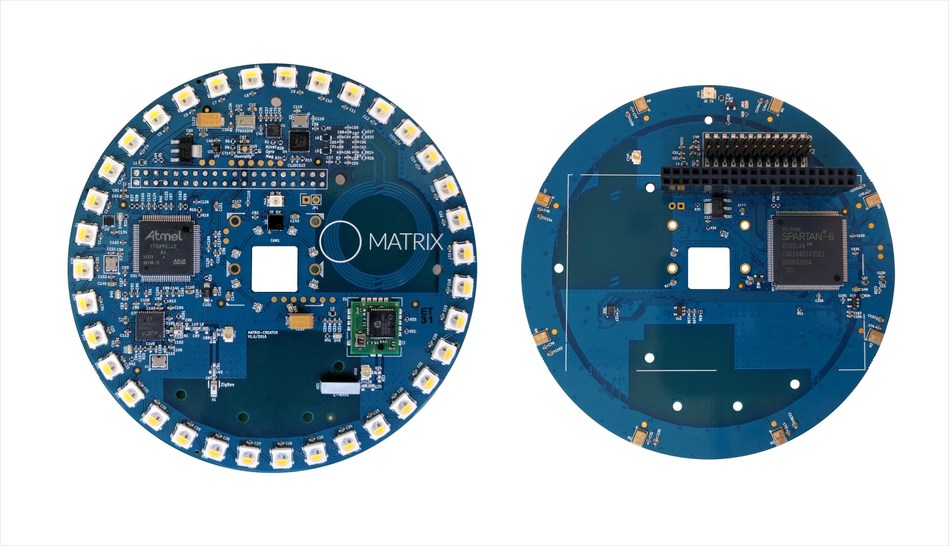
Distributor Premier Farnell has signed an exclusive partnership with MATRIX Labs for its Raspberry Pi add-on that provides multiple functionality and enables faster and more cost-effective development of IoT devices.

MATRIX Creator aimed at the development of applications in automation control systems, particularly for home automation systems involving optical and sound elements as well as robotics, enterprise logistics, voice assistants and beamforming/DoA algorithms. 

The development board, designed for Raspberry Pi, incorporates a Xilinx Spartan 6 FPGA, an ARM Cortex M3 microcontroller, a range of sensors for motion, temperature, humidity, light, ultraviolet and infrared, an 8-microphone array and a 35-LED array.

The microphone array, for example, allows a user to develop their own "do it yourself" Amazon Echo and Alexa based projects as well as voice recognition systems, with the eight microphones allowing devices to be activated from anywhere in a room. Similarly, the optical and physical sensors enable the development of facial recognition and motion detection devices for security applications.

"MATRIX Creator is a hugely exciting product, doing for the Internet of Things and artificial intelligence, what smartphones did for the mobile revolution," said Rodolfo Saccoman, CEO and Co-Founder of MATRIX Labs. "It has deep product functionality and we expect broad appeal - it's the perfect combination of an easy-to-use yet also sophisticated dev board, which appeals to the maker, the expert developer, and everyone in between. MATRIX Creator allows developers of virtually any skill-level to create whatever exists in their mind's eye, shifting the product development paradigm from one that relies on a 3rd party to create for you, to one where you can create the custom app that meet your exact needs. It's putting power into the hands of the people and democratizing IoT app development."
MATRIX Creator pioneers the use of machine intelligence as a building block for hardware. The $99 sensor-packed development board and platform allow developers to build IoT apps quickly and inexpensively for drones, robots, smart homes, security, gaming, retail, and whatever idea they imagine. 

The system can also be for hardware development and provides expert users with an extremely versatile piece of hardware to add to their suite of development tools. It accelerates and reduces the overall cost of the prototyping process for new products and devices, doing the up-front heavy lifting so developers don't have to.

The board, which can be programmed in 40 different languages, also incorporates integrated Z-Wave and Zigbee communications plus connectivity via a wide range of analogue and digital input/output interfaces. It can also be used in stand-alone mode using its onboard processing capability. 

"As the Development Distributor we work to source the latest innovative technology to help create opportunities for our existing and future builders, developers, makers and engineers," said Ralf Buehler, Senior Vice President, Sales and Marketing at Farnell. "Products like MATRIX Creator provide huge flexibility to users - unlike existing add-ons which only provide individual elements of functionality, MATRIX Creator is a complete development eco-system that allows users to access a range of functionality to enhance any Raspberry Pi based project, speeding up the design process and helping to overcome the hurdles involved in the creation of innovative hardware projects."

Friday, June 23, 2017

Researchers develop a lens-less ultra-thin camera

By Nick Flaherty www.flaherty.co.uk


Researchers at Caltech have developed an ultrathin camera sensor that doesn't need a lens to provide focus, opening up the possibility of dramatically thinner embedded designs.

The key to the sensor is an optical phased array (OPA) that computationally does what lenses do using shaped pieces of glass or plastic.

The OPA has an 8x8 array of light receivers, each of which can individually add a tightly controlled time delay (or phase shift) to the light it receives, enabling the camera to selectively look in different directions and focus on different things with large amounts of digital signal processing (DSP).

"Here, like most other things in life, timing is everything," said Ali Hajimiri, Bren Professor of Electrical Engineering and Medical Engineering in the Division of Engineering and Applied Science at Caltech, and the principal investigator. "With our new system, you can selectively look in a desired direction and at a very small part of the picture in front of you at any given time, by controlling the timing with femto-second--quadrillionth of a second--precision,"  

"We've created a single thin layer of integrated silicon photonics that emulates the lens and sensor of a digital camera, reducing the thickness and cost of digital cameras. It can mimic a regular lens, but can switch from a fish-eye to a telephoto lens instantaneously -- with just a simple adjustment in the way the array receives light," he said.

A similar principle to a phased array antenna is used in reverse in an optical phased array receiver. Light waves that are received by each element across the array cancel each other from all directions, except for one. In that direction, the waves amplify each other to create a focused image.

"What the camera does is similar to looking through a thin straw and scanning it across the field of view. We can form an image at an incredibly fast speed by manipulating the light instead of moving a mechanical object," says graduate student Reza Fatemi.

Last year, Hajimiri's team developed a one-dimensional version of the camera that was capable of detecting images in a line, such that it acted like a lensless barcode reader but with no mechanically moving parts. This first 2D lensless camera has an array composed of just 64 light receivers, limiting the resolution, but represents a proof of concept for a fundamental rethinking of camera technology says Hajimiri.

"The applications are endless," says graduate student Behrooz Abiri. "Even in today's smartphones, the camera is the component that limits how thin your phone can get. Once scaled up, this technology can make lenses and thick cameras obsolete. It may even have implications for astronomy by enabling ultra-light, ultra-thin enormous flat telescopes on the ground or in space."

"The ability to control all the optical properties of a camera electronically using a paper-thin layer of low-cost silicon photonics without any mechanical movement, lenses, or mirrors, opens a new world of imagers that could look like wallpaper, blinds, or even wearable fabric," said Hajimiri. 

Naturally the team is now working on scaling up the camera by designing chips that enable much larger receivers with higher resolution and sensitivity.


Related stories: