All the latest quantum computer articles

See the latest stories on quantum computing from eeNews Europe

Thursday, March 31, 2011

German company launches first commercially available automated software for process ports

By Nick Flaherty www.flaherty.co.uk

Automated Schematic Porting Tool Cuts Effort by 10-100X Compared to Manual Porting
 MunEDA in Munich has launched the first commercially-available electronic design automation (EDA) software tool to automate the time-consuming task of porting circuit schematics and intellectual property (IP) between different process technologies and process design kits (PDKs). 
As the newest member of MunEDA’s tool suite, the WiCkeDTM SPT Schematic Porting Tool executes 10-100X faster than manual schematic porting, significantly reducing design time and effort. The tool supports migration paths in major TSMC process technologies such as from tsmcN65 (65nm) to tsmcN40 (40nm), but can be configured also for different process migration paths. 
“IP and schematic porting is one of the key topics of the industry,” said Andreas Ripp, MunEDA vice president Sales & Marketing. “Migrating circuit schematics between different process technologies and PDKs can be a very time-consuming task for circuit designers, and we see a clear customer need for an automated solution. MunEDA invested in the development of this advanced technology and methodology, which significantly increases designer productivity and is much simpler than manual schematic porting.”
MunEDA WiCkeD SPT supports designers with an efficient design migration path, automatically replacing cells in the source PDK with corresponding cells for the target PDK. It provides flexible property mapping and automated shrinking, and handles all kinds of devices such as MOS transistors, resistors, capacitors and others. It is configurable for many source and target process technologies, and is initially available in TSMC processes. MunEDA can set up further process technologies on request. MunEDA WiCkeD SPT is fully integrated into the Cadence Virtuoso-based unified custom/analog flow.
“SPT addresses the ever-growing challenge of migrating many design blocks – and even entire SoCs – from one process to another in a short time, often with limited engineering capacity," said Michael Pronath, MunEDA vice president of Products & Solutions. "Migrating analogue/mixed-signal (AMS) designs, RF designs, IP libraries and high-speed interfaces is particularly challenging, because there is no simple rule for shrinking them. Most blocks need individual adjustment of topology, geometries, biasing, etc., even if the specifications don’t change. It is therefore necessary to migrate and port the schematics individually to conform to the technology constraints and to meet performance specifications. Manual migration is effort-intensive, and threatens to be a bottleneck. SPT solves these problems.”
MunEDA WiCkeD SPT will begin shipping in April. Pricing for a single license starts at $25,000 USD for a one-year time-based license.
Enhanced by Zemanta

Monday, March 28, 2011

MIPS to develop multi-threaded 64bit multiprocessor core


“Prodigy” core for Advanced Networking, Storage and Mobile

By Nick Flaherty www.flaherty.co.uk

MIPS Technologies plans to offer the industry’s first IP core that combines a 64bit processor architecture with simultaneous multi-threading (SMT) technology. The core, the first in a family of cores code named “Prodigy,” will be officially launched later in 2011. By offering the combination of a 64bit architecture, SMT technology and coherent multiprocessing in an off-the-shelf IP core, MIPS is providing the mass market with a fast path to performance, efficiency and scalability for advanced networking, storage, mobile and digital consumer designs.
Unlike ARM, MIPS Technologies has a long history in 64bit processing. The company has licensed its MIPS64 architecture to numerous licensees for a range of embedded markets including advanced networking, storage and servers, where applications can benefit from the larger address space and increased data processing capability of a 64bit architecture. MIPS Technologies also has an extensive history in multi-threading technology. Multiple MIPS licensees have reported significant increases in performance as well as overall system efficiency with MIPS-Based multi-threaded processors. SMT promises even higher gains in performance and efficiency through the ability to execute multiple instructions from multiple threads every clock cycle.
“With MIPS Technologies’ deep expertise and tradition in both multi-threading and 64bit processing, this is a natural next step,” said Joseph Byrne, an analyst at The Linley Group and author of A Guide to CPU Cores and Processor IP. “As applications become more complicated and require more memory, there is a basic limitation of accessing memory with 32bit addresses. That limit is becoming a barrier. Ultimately it will be necessary for many embedded applications to move to 64bit architectures because of the practically unlimited address space they allow. The time is right for MIPS to introduce this product to the market, because the next generation of advanced communications and networking products will need this headroom.”
“With our forthcoming core, our customers can now quickly and easily develop MIPS64 solutions at a fraction of the cost and time it would take to develop a 64bit core themselves,” said Art Swift, vice president of marketing and business development, MIPS Technologies. “We’re pleased to offer this solution, for which we are seeing increasing demand. Our customers can leverage not only the advanced 64bit Prodigy IP core, but they will also benefit from the surrounding infrastructure and broad, mature ecosystem that are already in place for the MIPS64 architecture as well as multiprocessing and multi-threading on MIPS.”
The Prodigy core family will offer seamless code compatibility and an elegant upward migration path between the MIPS32 and MIPS64 architectures.
Enhanced by Zemanta

Thursday, March 24, 2011

ST launches Next-Generation iNEMO engine

Enables New Level of Motion-Sensing Applications on Smart Consumer Devices

By Nick Flaherty www.flaherty.co.uk


STMicroelectronics has unveiled the first details of its new iNEMO sensor engine.

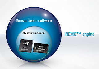
The advanced filtering and predictive software engine integrates the outputs from a 3-axis accelerometer, 3-axis gyroscope and 3-axis magnetometer. Fusing these sensors’ data, the iNEMO delivers dramatically more accurate and reliable sensor performance for next-generation smart consumer devices for a host of new motion-based applications.
For many current applications, such as freefall detection, screen rotation or pedometers, a single MEMS accelerometer meets their system requirements. However, a new class of advanced applications is emerging, for example: location-based services, enhanced motion-based gaming, pedestrian dead-reckoning for indoor and multi-floor navigation, robotics or human-body tracking. These applications require multiple MEMS sensors, together with advanced software, to achieve better overall system performance in terms of accuracy, resolution, stability and response time.
“The iNEMO Engine delivers a quantum leap in the performance level required by next-generation smart mobile devices to enable a myriad of new exciting applications,” said Benedetto Vigna, Group Vice President and General Manager of ST’s MEMS, Sensors and High Performance Analog Division “It also lifts the burden of complex sensor algorithm development off the shoulders of our customers.”
The iNEMO Engine software integrates a set of highly sophisticated adaptive algorithms for prediction and filtering. The software takes data from the outputs of various motion sensors in smart consumer devices and integrates it so that the sensor outputs augment each other, leapfrogging what individual sensors can do alone. The software can correct for magnetic distortions registered on the magnetometer, dynamic distortion measured by the accelerometer, and inherent drift over time of the gyroscope. This protects the accuracy of heading information, removes pointing inaccuracies and drift problems, and virtually eliminates timeouts for calibration.
The iNEMO Engine is available now to major consumer manufacturers, upon request via the usual ST sales channels, for integration into leading mobile platforms in a two-chip sensor solution (LSM303DLHx e-compass and the L3G4200D gyroscope). Advanced new mobile devices using ST’s iNEMO Engine multi-axis sensors are expected to be in production at leading consumer manufacturers before the end of the year.
In addition, ST’s has a wide range of highly accurate MEMS sensors available for the iNEMO Engine. These sensors include accelerometers to measure linear acceleration and earth gravity, gyroscopes to measure angular velocity, and magnetic sensors that output reliable heading information.
Enhanced by Zemanta

ST launches Next-Generation iNEMO engine;

Enables New Level of Motion-Sensing Applications on Smart Consumer Devices

By Nick Flaherty www.flaherty.co.uk


STMicroelectronics has unveiled the first details of its new iNEMO sensor engine.

The advanced filtering and predictive software engine integrates the outputs from a 3-axis accelerometer, 3-axis gyroscope and 3-axis magnetometer. Fusing these sensors’ data, the iNEMO delivers dramatically more accurate and reliable sensor performance for next-generation smart consumer devices for a host of new motion-based applications.
For many current applications, such as freefall detection, screen rotation or pedometers, a single MEMS accelerometer meets their system requirements. However, a new class of advanced applications is emerging, for example: location-based services, enhanced motion-based gaming, pedestrian dead-reckoning for indoor and multi-floor navigation, robotics or human-body tracking. These applications require multiple MEMS sensors, together with advanced software, to achieve better overall system performance in terms of accuracy, resolution, stability and response time.
“The iNEMO Engine delivers a quantum leap in the performance level required by next-generation smart mobile devices to enable a myriad of new exciting applications,” said Benedetto Vigna, Group Vice President and General Manager of ST’s MEMS, Sensors and High Performance Analog Division “It also lifts the burden of complex sensor algorithm development off the shoulders of our customers.”
The iNEMO Engine software integrates a set of highly sophisticated adaptive algorithms for prediction and filtering. The software takes data from the outputs of various motion sensors in smart consumer devices and integrates it so that the sensor outputs augment each other, leapfrogging what individual sensors can do alone. The software can correct for magnetic distortions registered on the magnetometer, dynamic distortion measured by the accelerometer, and inherent drift over time of the gyroscope. This protects the accuracy of heading information, removes pointing inaccuracies and drift problems, and virtually eliminates timeouts for calibration.
The iNEMO Engine is available now to major consumer manufacturers, upon request via the usual ST sales channels, for integration into leading mobile platforms in a two-chip sensor solution (LSM303DLHx e-compass and the L3G4200D gyroscope). Advanced new mobile devices using ST’s iNEMO Engine multi-axis sensors are expected to be in production at leading consumer manufacturers before the end of the year.
In addition, ST’s has a wide range of highly accurate MEMS sensors available for the iNEMO Engine. These sensors include accelerometers to measure linear acceleration and earth gravity, gyroscopes to measure angular velocity, and magnetic sensors that output reliable heading information.
Enhanced by Zemanta

Wednesday, March 23, 2011

Corning sees displays embedded everywhere in the home

By Nick Flaherty www.flaherty.co.uk

A video from Corning has an interesting view of the future for touchscreen displays embedded into a range of household items such as bathroom mirrors and kitchen work surfaces, with an optimistic 'near future' view!

ZTE shows record-breaking 10Tbit/s data link

Push to 400Gbit/s systems drives need for 10Gbit/s trunking

By Nick Flaherty www.flaherty.co.uk

Chinese telecoms equipment maker ZTE has broken the previous world record for single-channel data transmission with a recorded single-channel rate of 10Tbit/s over 640km of single-mode fibre optic cable. This is the equivalent of sending 160 HD movies per second.
The results of the test transmission were presented at the recent OFC/NFOEC conference in Los Angeles and lays a foundation for future research into optical transmission technology with higher single-channel rates at the heart of the internet of the future based on ZTE's patented  “carrier generation technology”. This generates 112 coherent and frequency-locked optical sub-carrier signals; with each sub-carrier bearing 100Gbit/s optical signals, and successfully achieved optical signals with a single-channel rate of 11.2Tbit/s, a net 10Tbit/s line rate plus overheads such as forward error correction (FEC).
In an era where the global optical communications industry is entering 100Gbit/s transmission, all mainstream manufacturers are not only promoting the practical deployment of 100Gbit/s but also actively seeking candidate technologies at higher bit rates of 400Gbit/s, 1Tbit/s, and beyond. With rapid growth in demand for higher bandwidth, single channel 10Tbit/s will be the transmission rate for future telecommunication networks.
The ZTE paper was the only post-deadline paper presented by a Chinese company at the conference and the company sees this as confirming its position as a global technology leader in the fibre communications transmissions over competitors such as Huawei.
“With OFC’s acknowledgement of our research results in 100G and beyond-100G technology, we will go on to invest further efforts in high-speed optical transmission and apply further research results in the pending global deployment of 100G technologies,” said Fan Xiaobing, General Manager of ZTE’s bearer network product line.

Enhanced by Zemanta

Friday, March 18, 2011

Solid State Drives Boom in 2011

Twin engines of consumer and enterprise usage will fuel growth to over $4bn

By Nick Flaherty www.flaherty.co.uk

Have we finally turned the corner to see solid state drives start to really take off? IHS iSuppli thinks so, predicting a near doubling of revenues this year to hit more than $4 billion and extending a robust performance in the storage market for the second year in a row.
SSD revenue this year is projected to hit $4.4 billion, up 91.3 percent from $2.3 billion in 2010. Growth in 2011 continues the expansion of the market starting last year, when the industry crossed the $1 billion threshold, figures indicate. This is becoming more apparent with SSD maker OCZ buying controller chip designer Indilinx this week.SSD revenue will continue to push ahead in the near future, even though the succeeding years will yield less impressive growth rates ranging from 7 to 25 percent. By 2014, SSD revenue is anticipated to reach $7.2 billion.


Ramping up in Consumer and Enterprise Segments
A number of compelling factors this year is spurring growth in SSDs—a type of storage technology comprised mostly of semiconductors and without any movable parts, unlike their rival hard disk drives made of magnetic media. Not only has pricing dropped for the NAND flash memory chips used in SSDs, solid state drives also are picking up real traction in both the consumer and enterprise markets.
The industry’s hottest segment in 2011 will be SSDs for consumer usage, IHS predicts, as shipments of SSD-outfitted high-end notebooks skyrocket. Last year’s Apple Inc.’s MacBook Air, for instance, succeeded in highlighting the SSD as a tangible differentiator—as opposed to soft attributes like design and build quality—for high-end notebooks. By designing around a small storage footprint and throwing in the fast performance typical of NAND flash, Apple delivered an attractive computing experience otherwise not achievable through a hard drive, thereby demonstrating the virtues inherent in SSD-equipped computers.
SSD’s other growth segment this year lies in the enterprise, which increasingly employs flash storage to overcome performance bottlenecks. In applications like online transaction processing and financial analysis, SSD drives using single-level-cell (SLC) NAND are preferred in order to enable optimal bandwidth and longevity. In addition, “enterprise-grade” multi-level-cell (MLC) NAND flash also has picked up steam as vendors improve MLC performance and controller sophistication, with a majority of enterprise SSDs now shipping with MLC flash.
Boosting SSD’s cachet within the enterprise segment, transformative applications—such as tiered server and storage system designs—are occurring, made possible by solid state technology. Other new applications capitalizing on the advantages of NAND flash also are getting ready to take off, further distancing SSDs from their hard disk drive legacy.
IHS revenue prospects for SSD this year have been consistent with last year’s outlook, but the sentiment then wasn’t as buoyant coming on the heels of a slow first half. SSDs had struggled earlier in 2010—partly due to a rise in NAND prices, and also because hard disc drives continued to increase their capacity and price advantage. But now, given the star turn for SSDs in ultraportable notebooks as well as an enhanced profile in the enterprise, the success projected by IHS for the industry has become a reality.
Mirroring the notable results in revenue, SSD shipments this year will be on an upswing, projected to reach approximately 15 million units, an increase of more than 118 percent from 6.9 million in 2010. Yet SSD shipments remain miniscule compared to those for hard disk drives, which will total roughly 161 million units in the first quarter of 2011 alone. At the same time, the hard disk drive market is consolidating and seeing much slower growth.

Read More > SSD Boom in 2011 Fueled by Twin Engines


Enhanced by Zemanta

Planning not panic is the key to IPv6 migration

By Nick Flaherty www.flaherty.co.uk

Duncan Hughes, systems engineering manager at Brocade recommends a 6 Step Systematic approach to  issue of migrating from IPv4 to the new generation IPv6 addresses. With IPv4 addresses down to the last few blocks, many are asking whether fears that IPv6 is the ‘end of the Internet’ is nothing more than vendor induced hype, or if it is something network managers and CIOs need to take seriously.
Brocade argues that while IPv6 migration is a serious issue that needs action, it is not a reason to panic and that phased deployments can reduce both the financial and performance impact on the enterprise. It recommends a 6 Step approach to IPv6:

1. Don’t Panic, PrepareWhile there is no need for panic, IPv6 is something businesses need to start preparing for - and preparing for right now. Understand the impact on your business

2. Conduct an in-depth Audit of your networkThe question isn’t ‘are you IPv6 ready?’ but ‘WHERE are you IPv6 ready?’ IT companies have been offering IPv6-ready solutions for some time, and some applications and services are less likely to be impacted. Those that are customer facing and mission critical should be the priority.

3. Create a strict timeline, and stick to itIt will take a while before the number of IPv6 addresses issued generates a ‘tipping point’ - estimates suggest it will be another 12 months before the available IPv4 addresses completely run out. But as the number of Internet users continues to increase (up to 1.97 billion in 2010, a year on year increase of 14 percent), it won’t be long before IPv6 use grows to a level that creates problems.

4. Don’t try and do everything at once If a full network upgrade is under consideration, this is a good to time to clean-house. If not the best approach is one of incremental migration over time versus any ‘rip and replace proposition’ (a high cost and high risk approach)

5. Recognise that the network needs to support your business demands today, tomorrow and in the future for your business to succeedPlan your migration in a series of stages to reduce impact on business activities, and see it as part of a long-term network evolution. Build your IPv6 planning into product lifecycle replacement plans and don’t consider anything that isn’t compatible with IPv6 moving forward

6. Recognise that interim solutions can provide long-term ROIUsing transition technologies such as double stacks, will help manage the initial flow of IPv6 traffic, and don’t dismiss translation solutions. Upcoming new solutions mean you can run IPv6 and IPv4 without any noticeable time-lag. Diligently review the solutions available before taking action. There are dual-protocol point-solutions available that are specifically engineered to help organisations make the transition without the need for costly upgrades.
Enhanced by Zemanta

Wednesday, March 16, 2011

Graphics-Enabled Microprocessor Use Surges in 2011

By Nick Flaherty www.flaherty.co.uk

This year will be the biggest period yet for graphics-enabled microprocessors (GEM), as the penetration of GEMs reaches 50 percent in notebook PCs and 45 percent in desktops, says the latest research from IHS iSuppli.

This will also drive the use of GEMs in embedded systems bringing more sophisticated graphics and user interfaces without the power consumption, cost and complexity of separate graphics cards.

Global GEM penetration in the notebook segment in 2011 will rise by a dramatic 11 percentage points from 39 percent in 2011. With worldwide notebook shipments expected to amount to more than 230 million units this year, GEMs will be in about 115 million notebooks by the end of 2011.

For desktops, GEM penetration this year will increase by a robust 9 percentage points from 36 percent in 2011. With desktop PC shipments experiencing a resurgence in 2010 and 2011 thanks to strong corporate replacement demand, IHS expects shipments of GEM-equipped desktop PCs to exceed 63 million in 2011.

By 2014, 83 percent of all notebook PCs and 76 percent of desktop PCs worldwide will ship with GEMs.

“GEMs are microprocessors that feature a central processing unit (CPU) as well as a graphics processing unit in a single-chip design, supplementing the brains of a PC with more graphics capability to run visually intensive applications,” said Peter Lin, principal analyst for compute platforms at IHS. “With GEMs capable of generating the total graphic output of a PC, no additional graphics processor or add-in graphics card is needed. Computers today are serving up ever-richer multimedia experiences, so the graphics capabilities of PCs have become more important, driving the rising penetration of GEMs.”

Intel vs. AMD
The two biggest players in the PC microprocessor field, Intel and Advanced Micro Devices (AMD), are intensifying their competition in the GEM market in 2011, IHS iSuppli research indicates. Intel at the beginning of 2011 was getting ready to launch its second-generation Core processor family known as Sandy Bridge, which integrates the CPU and graphics processor into one single piece of silicon. AMD, on the other hand, will release five application platforms with five GEM microprocessor categories.

The third player, VIA, caters to different markets with GEM solutions for embedded and industrial applications.
GEMs vs. discrete graphic cardsDespite their rising popularity, GEMs are unlikely to offer the same high level of performance as discrete graphics cards, IHS believes. Discrete graphics cards will remain the solution of choice for leading-edge graphics, providing high-end performance for applications such as games. In comparison, GEMs could be used to satisfy the needs of the mass PC market that does not require high-level graphics functionality, with the product targeted at the mainstream and value PC segments.
As a result, while some cannibalization of the discrete graphics market will occur because of GEMs, erosion of the discrete market will not be significant in the short to medium term, IHS believes.
Enhanced by Zemanta

Chipworks reverse engineers the Apple A5 processor

By Nick Flaherty www.flaherty.co.uk

Chipworks has reversed engineered the Apple A5 processor used in the iPad2. 
They decapsulated the A5 a couple of days ago, but as you could see in those early pictures, you can’t tell much of a chip’s layout from the top metal – it’s all power and ground buses.  So they had to de-layer the chip down to a level to see the block layout of the chip; not an easy thing when there’s nine layers of metal!  In fact, these days it’s easier to go in from the back and remove the substrate silicon, and look at the gate level from below.  Then they identify the circuit blocks that make up the full device.
For the A5, a dual ARM core processor:
Apple A5 Polysilicon Die Photo with Annotations
The ARM cores are in the right half of the die, with ~4.5 Mb of cache memory each.  You can also see the USB interface at the top, and the DDR SDRAM interfaces at the bottom right, for the memory in the top part of the package-on-package.  Other I/O blocks are strewn around the edge of the die.
It seems likely that Apple will actually be shipping TSMC-made parts later this year, since Samsung is a competitor with its Galaxy tablet series, but the current devices are made by Samsung, as shown by a cross section of the chip:

Enhanced by Zemanta

Tuesday, March 15, 2011

Microcameras become disposable

By Nick Flaherty www.flaherty.co.uk

Researchers at the Fraunhofer Institute in Germany have developed a microcamera that is as small as a grain of salt and cheap enough to be disposable, opening up opportunities in medical and automotive applications.
Endoscopy has gone through amazing advancements in recent years. Microcameras on the tip of endoscopes supply images from the inside of the human body in ever higher resolution, which often makes it possible to identify tumors at an early stage. Endoscopes though have some downsides, since they are expensive and, because of their multiple usages, have to be put through time-consuming and exhaustive cleaning procedures every time they are used. 
This problem might be solved by the new microcamera that the Fraunhofer Institute for Reliability and Microintegration (IZM) in Berlin, Germany has developed together with Awaiba and with the support of the Fraunhofer Institute for Applied Optics and Precision Engineering IOF in Jena, Germany. 
“We can produce microcameras so inexpensively with our technology that doctors can dispose of endoscopes after using them only once,” said Martin Wilke, a scientist at the Fraunhofer Institute for Reliability and Microintegration. This is made possible by a new type of manufacturing process.
Digital camera systems consist of two components: a lens and a sensor that transforms the image into electrical signals. Electrical contacts on the sensor allow access to these signals and therefore also to the information of the image. Due to the way they are manufactured, these contacts are located between the sensor and the lens. The sensors are manufactured simultaneously in large numbers, like computer chips.
“You have to think of a book full of postage stamps where many thousand stamps are printed in one step," said Wilke. "If you want to use them, you have to separate one from another. Instead of a sheet of paper, with image sensors you have a circular disc of silicon that is known as a wafer.” 
About 28,000 image sensors fit onto one wafer and until recently, each and every one was sawed out, wired and mounted on the lens that was still missing. That means wiring them 28,000 times and mounting them just as often.
The researchers have streamlined this process by developing a new way to access the electrical contacts. Now, the wiring process is faster and the entire camera system is smaller. The trick lies in the fact that they do not reach the contacts of each individual image sensor via the side any more but rather, simultaneously, with all sensors via their reverse side while they are still connected as a wafer. 
That means that you no longer have to mount the individual lenses. Instead, you can connect them with the image sensor wafers as lens wafers. Only then is the stack of wafers sawed apart into individual microcameras. 
Another upside is the fact that it supplies razor-sharp pictures even with very thin endoscopes. To date, the camera systems built into them had to be divided because of their size. The lens was at the tip of the endoscope and the sensor at the other end of the glass fiber strand. The new microcamera is small enough for the tip of the endoscope. It has a resolution of 62,500 pixels and transmits the image information through the endoscope via an electrical cable and measures 1mm x 1mm x1mm.
It is not only medical technology, but also the automotive industry that is interested in this tiny camera. Presently, they are researching the possibility of replacing outside rearview mirrors on cars with microcameras. This would reduce flow resistance and energy consumption. Beyond this, installed in fittings, this camera would be able to calculate the driver’s eye movements and prevent him from nodding off for a few seconds. “Starting in 2012, using Fraunhofer’s expertise, we will be able to bring disposable endoscopes to market for only a few euros – we already have the prototype,” said Stephan Voltz, CEO of Awaiba.
Enhanced by Zemanta

Monday, March 07, 2011

Xilinx looks to 400Gbit/s network development

Virtex-6 HXT FPGA Platform Eases 100G Development and looks beyond

By Nick Flaherty www.flaherty.co.uk

In a stunning move, programmable chip maker Xilinx is looking at the development for 400Gbit/s systems with its latest generation of FPGAs, citing the rapid growth of video sharing and internet mobile platforms over both wireless and wired networks is driving insatiable demand for bandwidth. 
It has launched an Optical Transport Network (OTN) Targeted Design Platform for supporting faster market implementation of 100G line cards and demonstrating the key technology for a smooth path to the development of future 400G line cards based on its Virtex-6 HXT FPGA and says network operators and service providers are quickly pursuing 100G adoption and looking for next generation platform 400G line cards.
System architects can use the OTN platform to quickly demonstrate and evaluate the flexibility, high-end performance and integration capabilities of Xilinx FPGAs for 100G OTN applications. They can later smoothly migrate their designs to the Virtex-7 HT FPGA family to evolve to 400G line card applications.
"In order for the communications industry to effectively answer the insatiable demand for bandwidth, optical communications equipment vendors must deliver more rapidly and more effectively the necessary levels of flexibility, integration and performance without raising power consumption or costs into their optical platforms," said Krishna Rangasayee, Corporate Vice President and General Manager of Xilinx's Communications Business Unit. "As part of Xilinx's recent acquisition of Omiino, we have created a new OTN Solution Delivery Centre that will include all of Omiino's deep OTN expertise plus their existing portfolio of OTN solutions and OTN development platforms to give our customers the most optimized and cost effective solution for their systems."
Xilinx claims to have the only FPGA on the market with 10 Gbps optical jitter compliant receivers, giving the OTN Targeted Design Platform pre-defined and implemented reference designs for different OTN solutions, such as 100G ODU switching, 100G Ethernet to OTU4 transponders and 10x10 to OTU4 transponders. The OTN platform also includes integrated features for ease-of-use, such as highly optimized IP 100G MuxSAR solution developed by Omiino.
The OTN Targeted Design Platform is also using OTN IP cores from Xilinx Alliance Program Members. The OTN Targeted Design Platform is also interoperable with optical module vendors, such as Avago Technologies, and optical tester vendor, such as JDS Uniphase Corp.
"OTN is surging in popularity, and is replacing the role held by SONET/SDH as networks transition to 40G and 100G," said Andrew Schmitt, Directing Analyst for Optical at Infonetics. "Equipment manufacturers seek flexible approaches to implementing hardware in a rapidly changing and growing market, and are looking towards soft solutions such as the OTN IP that are now part of Xilinx's library of communications IP."
Virtex-6 HXT
System bandwidth needs continue to evolve and further optical system density is required for the move to 400G slots that will sustain infrastructure growth over existing networks. Designers using 40nm Virtex-6 HXT FPGA OTN solutions to meet 100G challenges today will be able to migrate their designs in the future to the 28nm Virtex-7 HT family to meet impending 400G demands. This portability is largely due to the unified architecture between Virtex-6 and Virtex-7 devices, which offer the only 28 Gbps optical jitter compliant FPGA transceivers to connect to CFP2 modules -- up to sixteen 28 Gbps transceivers and seventy-two 13.1 Gbps transceivers to connect up to four next generation CFP2 optical modules (4x100G).
Virtex-6 HXT FPGAs offer both 6.6Gbps GTX transceivers and 11.18 Gbps GTH transceivers to enable next-generation packet and transport, switch fabric, video switching and imaging equipment. The devices are built on 40nm process using a third-generation FPGA architecture at a 1.0v core voltage with an available 0.9v low-power option.
Virtex-7 HT
Built with four to sixteen 28 Gbps transceivers complying with OIF CEI-28G, the Optical Internetworking Forum's Common Electrical I/O specification for 28 Gbps, Virtex-7 HT devices are designed to interface to next generation CFP2 and QSFP2 optical modules that will be used in next generation 100 – 400G system line cards. The devices also have up to seventy-two 13.1 Gbps transceivers and can offer up to 2.8 Tbps full duplex throughput.

Pricing and Availability
The Virtex-6 HXT FPGA OTN Kit is $25,000 without optical modules and is available for order in April 2011.
Enhanced by Zemanta

Hard drive market consolidation continues as Western Digital acquires Hitachi GST in $4.3bn deal

Deal creates drive giant

By Nick Flaherty www.flaherty.co.uk

Western Digital is to acquire Hitachi Global Storage Technologies (Hitachi GST), a wholly-owned subsidiary of Hitachi, for approximately $4.3 billion. The deal creates a global giant that will outship the current #1 supplier, Seagate.

Apparently WD tried to buy Seagate late last year for a rumoured bid above $8bn while Seagate was in negotiation to sell to a private equity firm. The Hitachi deal gives WD the scale it need to compete and be sustainably profitable. The next challenge is managing the transition to Solid State Drives.     
"The acquisition of Hitachi GST is a unique opportunity for WD to create further value for our customers, stockholders, employees, suppliers and the communities in which we operate," said John Coyne, president and chief executive officer of WD. "We believe this step will result in several key benefits-enhanced R&D capabilities, innovation and expansion of a rich product portfolio, comprehensive market coverage and scale that will enhance our cost structure and ability to compete in a dynamic marketplace. The skills and contributions of both workforces were key considerations in assessing this compelling opportunity. We will be relying on the proven integration capabilities of both companies to assure the ongoing satisfaction of our customers and to bring this combination to successful fruition." 

"This brings together two industry leaders with consistent track records of strong execution and industry outperformance," said Steve Milligan, president and chief executive officer, Hitachi Global Storage Technologies. "Together we can provide customers worldwide with the industry's most compelling and diverse set of products and services, from innovative personal storage to solid state drives for the enterprise."

Hiroaki Nakanishi, president, Hitachi, Ltd. said, "As the former CEO of Hitachi GST, I always believed in the potential of Hitachi GST to become a larger and more agile company. This is a strategic combination of two industry leaders, both growing and profitable. It provides an opportunity for the new company to increase customer and shareholder value and expand into new markets. Additionally, it is important to us that WD shares common values with Hitachi GST to create a more global company that is well positioned to define a broader role in the evolving storage industry."

Deal details:
WD will acquire Hitachi GST for $3.5 billion in cash and 25 million WD common shares valued at $750 million, based on a WD closing stock price of $30.01 as of March 4, 2011. Hitachi will own approximately ten percent of Western Digital shares and two representatives of Hitachi will be added to the WD board of directors at closing. The transaction has been approved by the board of directors of each company and is expected to close during the third calendar quarter of 2011. WD plans to fund the transaction with a combination of existing cash and total debt of approximately $2.5 billion.

The resulting company will retain the Western Digital name and remain headquartered in Irvine, California. John Coyne will remain chief executive officer of WD, Tim Leyden chief operating officer and Wolfgang Nickl chief financial officer. Steve Milligan, president and chief executive officer of Hitachi GST, will join WD at closing as president, reporting to John Coyne.
Enhanced by Zemanta

Friday, March 04, 2011

Processing demand skyrocket as Wind River releases 64bit VxWorks

Improves multicore support for ARM and gives exclusive Intel primitives

By Nick Flaherty www.flaherty.co.uk

In a sign that 64bit processing is more clearly needed in embedded designs, Wind River has launched a 64bit version of its VxWorks real time operating system (RTOS).

Version 6.9 (although suprisingly this isn't VxWork7.0) is one of the first commercial RTOSes delivering 64bit computing support and includes improved multi-core processing support. 

“The embedded market is facing skyrocketing demands for processing performance as systems become ever more complex and increasingly connected. The sheer amount of compute power, memory and data required for embedded applications continues to climb exponentially,” said Warren Kurisu, vice president of VxWorks product management at Wind River. “By providing 64bit computing capability, Wind River addresses the high-performance needs of our embedded market. VxWorks continues to be an innovation leader that delivers vital solutions to our customers.”

VxWorks now delivers 64bit support both in data and code execution that was once the sole domain of supercomputer and server markets. For telecommunications network infrastructure equipment manufacturers, 64bit computing is critical in keeping up with the stresses of increasingly exploding data. Other vertical industries are also demanding 64bit support, for example, for industrial and medical applications such as high-definition imagery, and aerospace and defense applications such as highly complex radar, sonar and sensors. Companies already running VxWorks can rapidly transition to 64bit computing with ease.

The latest VxWorks delivers greater multi-core processing performance in both symmetric multiprocessing (SMP) and asymmetrical multiprocessing (AMP) configurations. VxWorks platforms now bundle the Intel optimizing C++ compiler and the Intel Performance Primitives (IPP) library for Intel architectures only. This version of VxWorks now includes support for the ARM Cortex A9 processor, with a multi-core SMP and ARM Thumb-2 instruction set. This VxWorks release also provides enhanced networking capabilities, including new security features and increased Internet Engineering Task Force Request for Comments (IETF RFC) support. Additionally, software development on VxWorks continues to be enabled by the Wind River Workbench development tools suite.
The latest version of VxWorks will be available this month.

Enhanced by Zemanta

Freescale Power Architecture microcontrollers for industrial market mark the end of ColdFire

By Nick Flaherty www.flaherty.co.uk

Freescale Semiconductor is moving its Power Architecture into microcontrollers that effectively marks the end of the ColdFire range for new designs.
The PX series of MCUs is based on Freescale’s e200 Power Architecture cores and is designed to meet the needs of the most complex industrial control applications, including motion control, power generation, clinical medical, aerospace and defence, motor drives, renewable energy, robotics and more.
“This addition to our industrial MCU portfolio is significant because the industrial electronics market can truly benefit from the capabilities of Power Architecture technology,” said Reza Kazerounian, senior vice president and general manager of Freescale’s Microcontroller Solutions Group. “The PX series of Power Architecture MCUs brings unparalleled performance to a broad range of industrial applications and provides the advanced technology and enablement our customers need for their industrial designs.”
The embedded safety architecture in the PX series of Power Architecture MCUs helps developers meet the safety, reliability and environmental requirements of industrial control applications. Integrated features simplify safety approvals for IEC61511 and IEC 61508 (SIL3), FAA DO-178B Level A and FDA Class II to III.
The single-core performance is up to 600 DMIPS, with multicore options and up to 4 MB of embedded flash memory make the PX series ideal for motion control and other complex, real-time control applications. A single chip can control up to six motors, process complex math algorithms and manage more than the typical three communications connections.
Freescale is also providing run-time software, reference designs and tools for rapid prototyping, advanced debug and system modelling. Customers can lower start-up costs by using Freescale run-time software, such as the free MQX RTOS, DSP and motor control libraries and Swell PEG (portable embedded GUI) development suite. Additionally, Freescale Power Architecture MCUs are supported by tools and the safety-certified INTEGRITY RTOS from Green Hills.
Freescale also offers tools for rapid prototyping with the PX series, including:
  • Modular Tower System hardware development platform with QuickStart code initialisation 
  • RAppID Toolbox with links to the MathWorks Simulink environment 
  • FreeMASTER debug GUI 
All families in the PX series are included in the Freescale product longevity program which ensures a minimum of 10 years of device availability (15 years for medical and automotive devices), providing peace of mind for the embedded designer. For more information, go to www.freescale.com/PXseries.


Related articles
Freescale Files for $1.15 Billion IPO (voices.allthingsd.com)
Freescale introduces intelligent sensor for car battery monitoring (physorg.com)
Freescale Boosts Share Of Tablet Processor Market (informationweek.com)